Metal sulfide nanomaterials have been a hot topic in the fields of solar energy conversion, optical electronic devices, catalysis, etc. They will play a more important role in the utilization of solar energy and optical electronic integrated circuits (OEIC) if their structure is properly designed and their thin films can be controllably synthesized and assembled.
The research group headed by Professor JIA Junhong at the State Key Laboratory of Solid Lubrication, Lanzhou Institute of Chemical Physics (LICP), Chinese Academy of Sciences (CAS), has controllably synthesized series of nanocrystalline metal sulfide (CuxS、CdS、In2S3 and Bi2S3) thin films on single-crystal silicon and FTO glass using chemical bath deposition(CBD) in combination with self-assembly technique. Furthermore, they have prepared complete and ordered patterned thin films applying self-assembly and violet lithography, and investigated the influence of pattern characteristics on the optical and photoelectric properties of thin films and also revealed the formation and growth mechanism of sulfide thin films.
The results show that the thin films prepared through self-assembly can be used as an effective template to control the crystal orientation, crystal shape recognition, surface morphology of metal sulfide nanomaterials. The thin films possess stable photocurrent and sensitive photoelectric response properties. The optical and photoelectric properties of thin films can be controlled by tuning the pattern size. These patterned functionalized thin films are expected to be applied in micro optical devices, sensors, solar energy cells, etc.
The work has received supports from National Natural Science Foundation of China. The findings have been published in CrystEngComm (2012, 14,3433), Journal of Colloid and Interface Science (2009, 332, 32-38; 2011, 356, 726-733.), ACS Appl. Mater. Interfaces (2010, 2, 3467–3472) and Applied Surface Science(2010, 256, 7316; 2011, 258, 649-656).
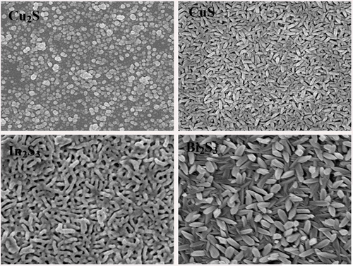
Surface morphology of metal sulfide thin film. (Image by JIA Junhong et al.)
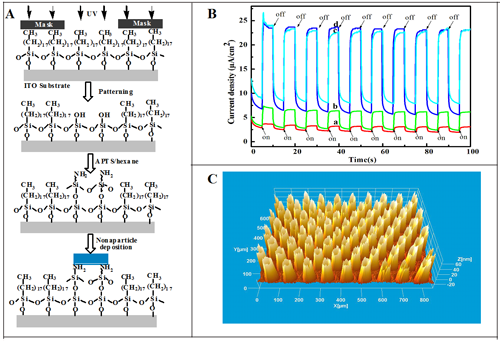
(A) Schematic diagram of the fabrication process for patterned Bi2S3thin films.(B)Photocurrent response of Bi2S3 thin films with differentreaction time. (C)3D surface images of patterned thin films.(Image by JIA Junhong et al.)
Journal of Colloid and Interface Science(2009, 332, 32–38)
Journal of Colloid and Interface Science(2011, 356, 726-733)
ACS Appl. Mater. Interfaces(2010, 2, 3467–3472)