Abstract
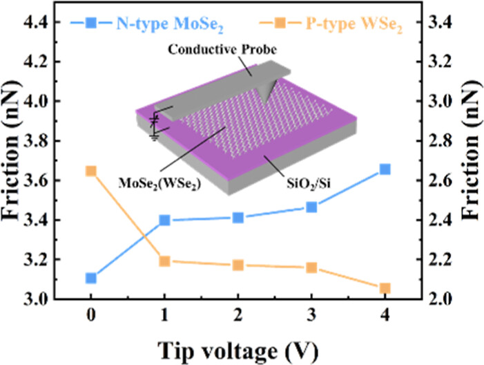
Nanofriction plays an important role in the performance and lifetime of n-type or p-type TMD-based semiconductor nanodevices. However, the mechanism of nanofriction in n-type and p-type TMD semiconductors under an electric field is still blurry. In this paper, monolayers of n-MoSe2 and p-WSe2 materials were prepared by chemical vapor deposition (CVD), and their nanofriction behavior under positive electric field was investigated. Atomic force microscopy (AFM) was used to analyze the nanofriction by the positive voltage applied through the needle tip: both the friction and the friction coefficient of MoSe2 increased with the increase of the applied voltage, while the friction and the friction coefficient of WSe2 decreased with the increase of the applied voltage. As the applied voltage increases, the friction force and energy dissipation exhibit corresponding trends in relation to the surface potential. The accumulation and dissipation of carriers represent significant factors influencing friction change. The diverse types of carriers give rise to variations in the friction laws. Our experiments have revealed the differences and mechanisms of friction in TMD materials dominated by different carrier types at positive voltages. It provides guidance for the application and modulation of n- and p-type two-dimensional semiconductor materials in the field of friction.

Published in ACS APPLIED MATERIALS & INTERFACES;10.1021/acsami.4c16577


